According to TrendForce, it has struggled with advanced process yield rates over the past few yearsSamsungIt seems that there has been a turnaround, and the next order worth 22.7 trillion won (about $16.5 billion) may change the direction of the foundry market. The agreement for the deal was signed on July 24, 2025, and the contract runs until December 31, 2033, equivalent to 7.6% of Samsung’s annual revenue, which may be the largest foundry order in Samsung’s history.

Although the customer information of the deal is confidential, soon Elon Musk (Elon).
Musk) revealed on its social media account that Samsung’s new fab in Tyler, Texas, USA, will be dedicated to manufacturing Tesla’s next-generation AI6 chips, confirming the deal from the side. It was later added that the deal could be worth much more than that.
In addition, Elon Musk also said,TSMC(TSMC) will first manufacture the newly designed AI5 chips in Taiwan, and then transfer them to the fab in Arizona, USA.
This contract is very encouraging for Samsung, at least the efforts in terms of yield rate have paid off. Samsung has lost to TSMC on the 3nm process node, and Tesla’s orders prove Samsung’s yield rate and technical strength on the 2nm process node, and third-party orders are expected to increase.
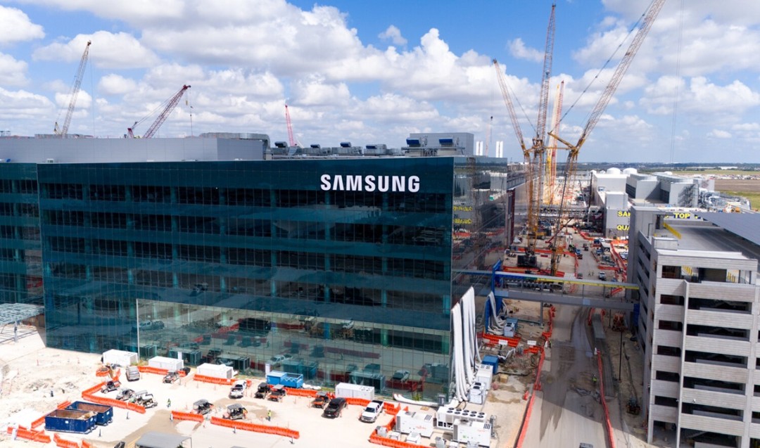
It was previously reported that Samsung began sending employees to the Taylor factory in the United States to restart local projects. These staff are responsible for handling the 3nm and below process and are expected to be set up and yield verified on-site in the U.S. according to the customer’s product specifications. Some industry insiders speculate that Samsung is trying to speed up the project progress and achieve mass production as early as the first quarter of 2026.